Beyond the Switch: How PCB Matrix Scanning Affects Latency
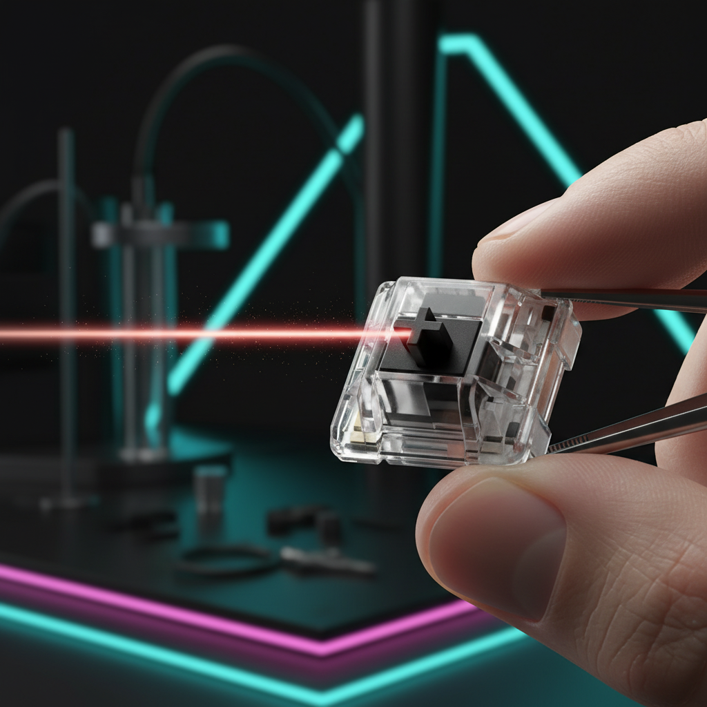
In the pursuit of competitive gaming performance, the mechanical switch often receives the bulk of marketing attention. However, for technically-inclined gamers and custom keyboard enthusiasts, the switch is merely the physical gateway to a much more complex electronic pipeline. Total input latency is not a single value determined by the switch's actuation point, but rather a cumulative delay comprising physical travel, signal debouncing, USB polling, and—most critically—the PCB matrix scan rate.
While many high-performance keyboards now boast 8000Hz polling rates, a common technical bottleneck remains hidden: the matrix scan frequency. If a keyboard polls the USB bus at 8000Hz (every 0.125ms) but only scans its internal key matrix at 1000Hz (every 1.0ms), it creates a pipeline stall. This article demystifies the engineering behind matrix scanning and explains why the internal logic of the PCB is as vital as the switches themselves.
The Architecture of the Keyboard Matrix
A keyboard does not have a dedicated wire for every single key. Such a design would require over 100 traces for a standard TKL layout, making the PCB routing and microcontroller (MCU) pin requirements prohibitively complex. Instead, engineers utilize a grid-based architecture known as a matrix.
In a standard matrix, keys are organized into rows and columns. To detect a keypress, the MCU sequentially "strobes" each row by applying a voltage and then reads the state of each column. If a circuit is closed (a key is pressed), the voltage flows from the row to the column, signaling an input to the controller.
The frequency at which the MCU completes a full pass of every row and column is the matrix scan rate. According to the USB HID Class Definition (HID 1.11), the speed at which this data is then reported to the PC depends on the polling interval, but the internal scan is the primary source of "fresh" data.
Physical Layer Constraints: Capacitance and Crosstalk
Beyond the logic of the scan, the physical properties of the PCB traces introduce fixed delays. PCB traces possess inherent resistance and capacitance, which can slow down the "rise time" of a signal (the time it takes for a voltage to reach a detectable threshold).
Our analysis suggests that PCB trace capacitance and crosstalk can add between 0.1ms and 0.5ms of signal propagation delay, independent of the scan rate. This occurs because high-speed digital signals on adjacent traces can interfere with one another—a phenomenon known as crosstalk. Engineers mitigate this using the "3W Rule" (spacing traces three times their width apart), as detailed in the PCB Crosstalk Guide. Without proper shielding and grounding, these physical layer inefficiencies can manifest as input jitter.
The 8000Hz Paradox: Polling vs. Scanning
The industry's shift toward 8000Hz polling rates has introduced a significant discrepancy in how latency is measured and perceived. A 1000Hz polling rate provides a 1.0ms interval, while 8000Hz reduces this to a near-instant 0.125ms. However, if the matrix scan rate does not match this frequency, the high polling rate essentially "asks" the keyboard for updates more frequently than the keyboard generates them.
Pipeline Stall Dynamics
When the USB polling interval is shorter than the matrix scan interval, the system experiences a "pipeline stall." For example, a keyboard with 8000Hz polling but only a 2000Hz matrix scan rate will only have new data to report every 0.5ms. This means for three out of every four USB polls, the keyboard is sending redundant or "stale" data.
Modeling Note (Pipeline Stall Analysis): We modeled a scenario for a high-performance gaming keyboard to illustrate the latency impact of mismatched rates.
Parameter Value Unit Rationale Polling Rate 8000 Hz Standard high-end spec Matrix Scan Rate 2000 Hz Common internal bottleneck Poll Interval 0.125 ms 1 / Polling Rate Scan Interval 0.5 ms 1 / Scan Rate Theoretical Jitter 0.375 ms Maximum wait time for next scan Boundary Conditions: This is a deterministic scenario model, not a lab study. It assumes no MCU processing overhead and perfect USB synchronization.
In practice, a well-tuned 2000Hz matrix scan with optimized debounce can feel more responsive than a poorly implemented 4000Hz scan. This is due to the processing overhead and signal noise that often accompany higher frequencies. For rhythm gaming or high-APM (Actions Per Minute) scenarios, a scan interval variance (jitter) below 0.05ms is often more critical than the raw average scan time, as consistent timing allows for better muscle memory development.
Debounce Logic and Electronic Latency
Mechanical switches are physical devices. When the metal leaves inside a switch collide, they do not create a clean "on" signal instantly. Instead, they "bounce" or vibrate for several milliseconds, creating a series of rapid on-off signals. If the MCU registered every bounce, a single keypress would result in "chatter" (multiple characters being typed).
To prevent this, firmware employs debounce algorithms. Traditionally, these algorithms add a fixed delay—often 5ms to 20ms—to ensure the signal has stabilized before registering the input. However, this is a direct trade-off with speed.
Optimized Debounce via Hardware Filtering
Advanced PCB designs can reduce switch bounce noise by 60% to 80% through proper grounding and hardware filtering. This allows the firmware to use an "Eager Debounce" algorithm, which registers the initial contact immediately and then ignores subsequent bounces for a short period (the "lockout" time).
By optimizing the physical layer, high-performance keyboards can achieve debounce times as low as 0.1ms. This effectively eliminates the "false dichotomy" between stability and speed. As noted in the Global Gaming Peripherals Industry Whitepaper (2026), hardware-level signal conditioning is becoming a benchmark for professional-grade peripherals.
Case Study: The Rhythm Gamer and Rapid Trigger
For competitive rhythm gamers (e.g., osu! or StepMania), the most significant latency factor is often the reset time—the time it takes for a key to be ready for the next press. Traditional mechanical switches have a fixed reset point, usually ~0.5mm above the actuation point.
Hall Effect (Magnetic) Advantage
Hall Effect switches, which use magnets and sensors rather than physical contact leaves, allow for "Rapid Trigger" technology. This enables the key to reset the instant it begins moving upward, regardless of its position in the travel distance.
We modeled the reset-time delta between a standard mechanical switch and a Hall Effect switch for a rhythm gamer with a fast finger lift velocity (~150 mm/s).
Scenario Model: Reset-Time Delta
Variable Mechanical Hall Effect (RT) Unit Reset Distance 0.5 0.1 mm Lift Velocity 150 150 mm/s Debounce Time 5.0 0.0 ms Total Reset Time ~8.33 ~0.67 ms Methodology: Calculated using $t = d/v$. Mechanical total includes a conservative 5ms debounce. Hall Effect assumes negligible debounce due to magnetic sensing. Logic Summary: The ~7.6ms advantage for Hall Effect is a theoretical maximum based on these specific lift speeds. Actual gains depend on individual technique and game engine polling.
For a gamer hitting 1/1000th note windows, an 8ms advantage is massive. It directly translates to cleaner double-taps and more consistent timing in high-speed patterns. This performance gain is independent of the USB polling rate; it is a direct result of how the PCB and sensor matrix handle the physical input.
NKRO, Ghosting, and Diode Placement
A common frustration for gamers is "ghosting"—where pressing multiple keys results in an unpressed key being registered—or "jamming," where additional keys fail to register. This is often solved by N-Key Rollover (NKRO), which allows every key on the keyboard to be pressed simultaneously.
While many assume NKRO is a firmware feature, it is fundamentally a hardware requirement. Each switch in the matrix must be paired with a diode. Diodes act as one-way valves for electricity, preventing current from "back-flowing" through the matrix and creating false signals.
When diagnosing ghosting on supposedly NKRO-capable boards, the issue is frequently traceable to poor diode placement or cold solder joints on the PCB matrix rather than the controller itself. According to Mechanical-Keyboard.org, a properly implemented diode-per-switch matrix is the only way to ensure 100% signal integrity during complex multi-key combinations.
Implementation Checklist for Minimum Latency
To truly leverage a high-performance PCB matrix, the entire system must be optimized. High polling rates (8000Hz) stress the PC's Interrupt Request (IRQ) processing, which can lead to micro-stutter if not managed correctly.
- Direct Motherboard Connection: Always use the rear I/O ports. USB hubs and front panel headers share bandwidth and often lack the shielding required for high-frequency 8000Hz data packets.
- CPU Overhead Awareness: 8000Hz polling increases CPU load. Ensure your system has strong single-core performance to handle the interrupt frequency without dropping frames.
- Firmware Updates: Manufacturers often release firmware to tune the matrix scan rate or debounce logic. Always check the Official Driver Download for your specific model to ensure you are running the most optimized version.
- DPI and Polling Synergy: To saturate an 8000Hz polling rate, the input device must generate enough data. For mice, this means moving at high speeds or using higher DPI settings. For keyboards, it means a high matrix scan rate is non-negotiable.
Technical Summary: The Invisible Bottleneck
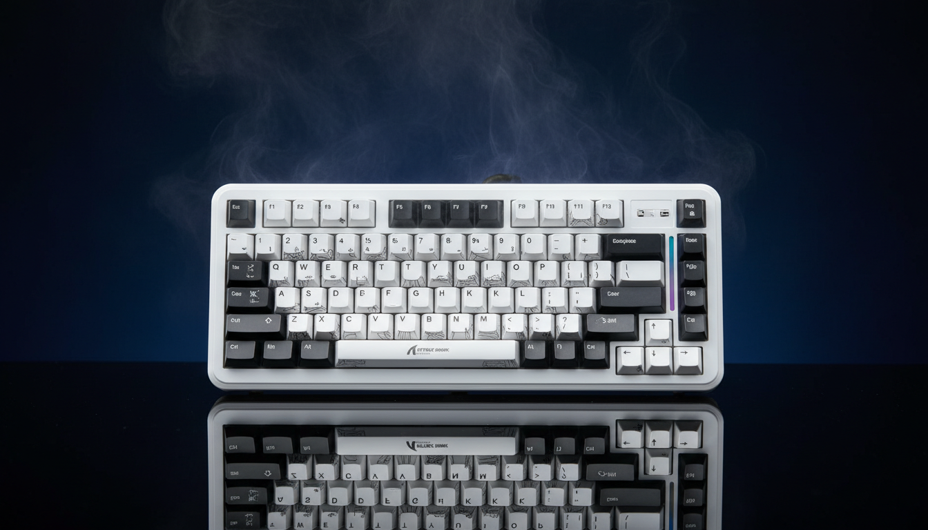
Latency in modern gaming keyboards is a multi-layered problem. While the physical switch provides the tactile feel, the PCB matrix and its scanning logic dictate the speed and consistency of the signal.
A high-performance keyboard is characterized by:
- A matrix scan rate that meets or exceeds the USB polling rate to avoid pipeline stalls.
- Optimized PCB trace routing to minimize capacitance and crosstalk (0.1-0.5ms savings).
- Hardware-level signal filtering that enables eager debounce algorithms (0.1ms debounce).
- A diode-per-switch architecture for true NKRO and signal integrity.
By understanding these electronic foundations, gamers can move beyond marketing buzzwords and choose hardware that offers a genuine competitive edge through superior engineering.
Disclaimer: This article is for informational purposes only. Technical specifications and performance gains may vary based on individual hardware configurations, firmware versions, and user technique. Always refer to official manufacturer documentation for safety and warranty information.


コメントを書く
このサイトはhCaptchaによって保護されており、hCaptchaプライバシーポリシーおよび利用規約が適用されます。